Schematic & layout
2–4 layer board design
PCB Design | Schematic & 2–4 Layer Layout
I’m an Automation and Control Engineering Technology graduate focused on PCB design, power supplies, component selection and board layout.
From schematic design and component selection to PCB layout.
Open to PCB Design Engineering opportunities.

 Codex
 Claude Code
2–4 layer board design
Power conversion fundamentals
Basic C/C++ and interfaces
Multimeter & oscilloscope
DESIGN WORKFLOW
Define board functions, interfaces, power needs and design constraints.
Check critical power and analog circuits where simulation is useful.
Select components, capture circuits and prepare the bill of materials.
Place and route components with stackup, return paths and manufacturing in mind.
Review design rules, electrical rules and key layout constraints.
Prepare fabrication outputs, BOM and assembly documentation.
Assemble and bring up the IoT Node prototype; other boards are design-complete.
Check board operation and troubleshoot with practical electrical test tools.
PCB design projects covering industrial power and embedded hardware.
ESP32-based IoT hardware for sensing, data logging and relay control.
STM32F407 controller for pump monitoring, VFD control and data logging.
Have a hardware challenge to explore?
↓ Download ResumePersonal PCB design projects, from schematics to board layout.
5 of 5 projects
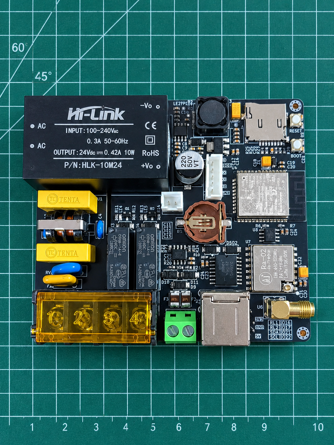
Integrated ESP32 IoT board with LoRa, RTC, microSD and two relay channels, powered by 220VAC.
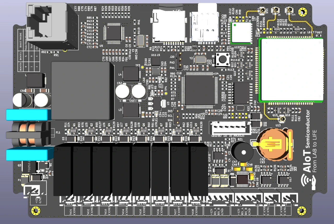
STM32F407-based controller for industrial pump monitoring, VFD control and data logging.
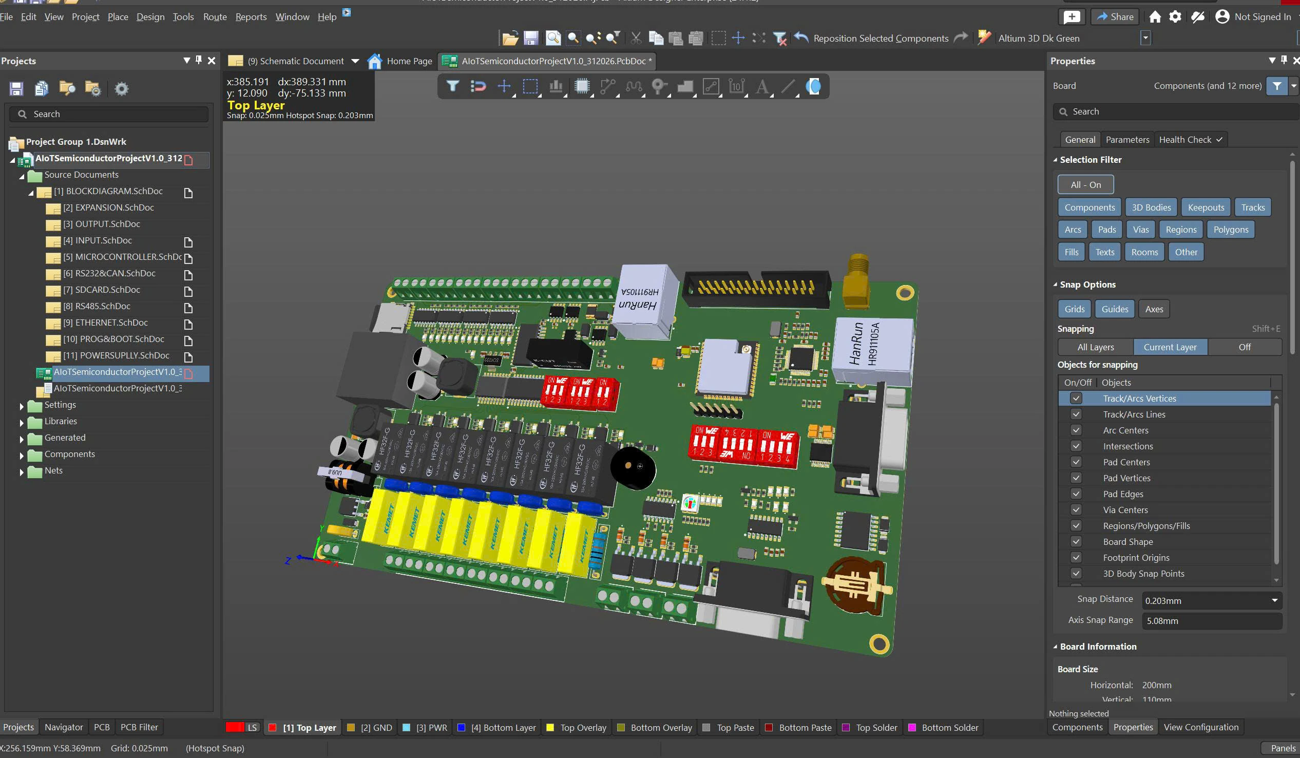
My personal ESP32 Datalogger hardware project, shown in Altium Designer.
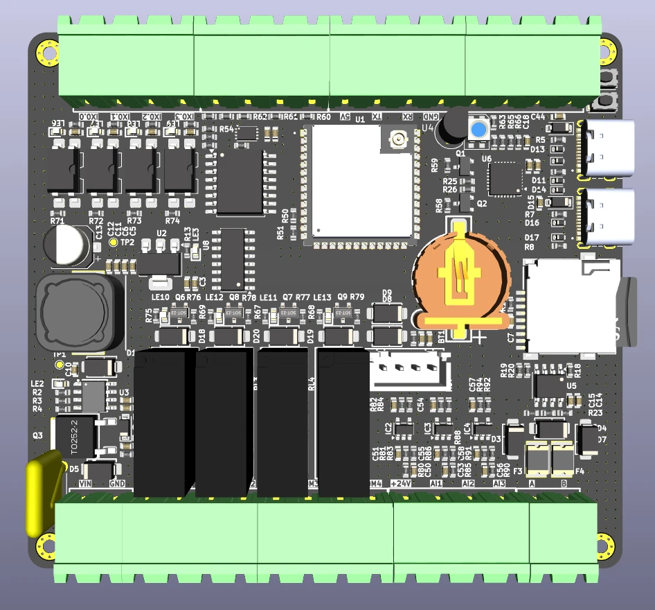
ESP32-S3 based PLC for industrial automation and IoT, with digital I/O, 4–20 mA analog interfaces and Modbus RS485.
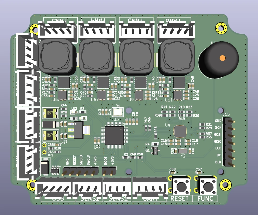
STM32F070-based intelligent PC fan controller with six PWM channels, four adjustable-voltage channels and USB control.
Personal PCB design projects by Hoàng Duy. Results reflect the completion status provided for each project.

I graduated in Automation and Control Engineering Technology from Ho Chi Minh City University of Technology and Engineering. My main focus is schematic design, component selection and 2–4 layer PCB layout.
I work with KiCad and Altium on power conversion and industrial board designs.
PCB design training, engineering education and electrical experience.
Schematic design, component selection, 2–4 layer layout and design-for-manufacturing basics.
Power conversion fundamentals and PCB design for multi-rail systems.
Industrial and board-level communication protocols.
Hands-on electrical testing and troubleshooting.
Wired and wireless connectivity used across board projects.
Basic C/C++ and familiarity with STM32 and ESP32 hardware.
PCB design tools, board layout and project documentation.
KiCad and Altium Designer for schematic capture and PCB layout.
Schematic design, component selection, 2–4 layer layout, stackup, routing, BOM and manufacturing outputs.
AC/DC and DC/DC conversion using Buck, Boost and LDO topologies.
I have basic C/C++ and hardware experience with STM32 and ESP32.
I2C, UART, SPI, CAN, RS232, RS485, Ethernet and USB.
Multimeters and oscilloscopes for practical electrical checks.
Discuss a PCB project or say hello. Explore my board designs, technical skills, or experience.