Schematic capture
Build circuits from symbols and wires, organize connections and check electrical consistency with ERC.
DESIGN TOOL / OPEN-SOURCE ELECTRONIC DESIGN
KiCad is a free, open-source electronic design suite. It connects schematic capture, PCB layout and board visualization in one project workflow, making it a flexible environment for learning, prototyping and developing electronic hardware.
FROM CIRCUIT TO BOARD
A closer look at the core functions used throughout an electronic design project.
Build circuits from symbols and wires, organize connections and check electrical consistency with ERC.
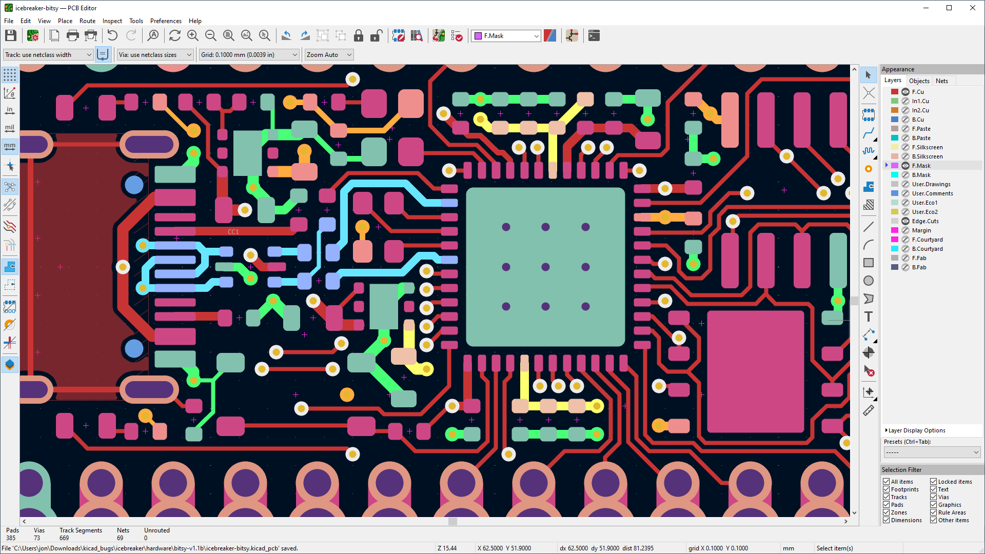
Place footprints and route copper with interactive routing modes that work with design rules.
Review clearances and layout conditions with configurable DRC checks before preparing a board for fabrication.
Work with symbols, footprints and matching 3D models; create custom library elements when needed.
Inspect the assembled board in the integrated 3D Viewer to better understand placement and physical form.
Update the PCB from the schematic and cross-probe between the two editors to locate components.
Continue learning with documentation from the software publisher.